600fA Input Noise Transimpedance Amplifier 140dB @ DC - 10kHz ±2.75V Dual Supply
Sold by Verdawave
The fTIA140-000 is a specialized ultra-low-noise transimpedance amplifier (TIA) module designed to interface directly with high-impedance low-frequency current sources, such as precision photodiodes, chemical sensors, or living biological material.
fTIA140-000 Product Specifications
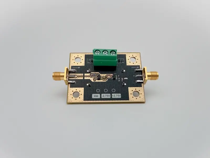
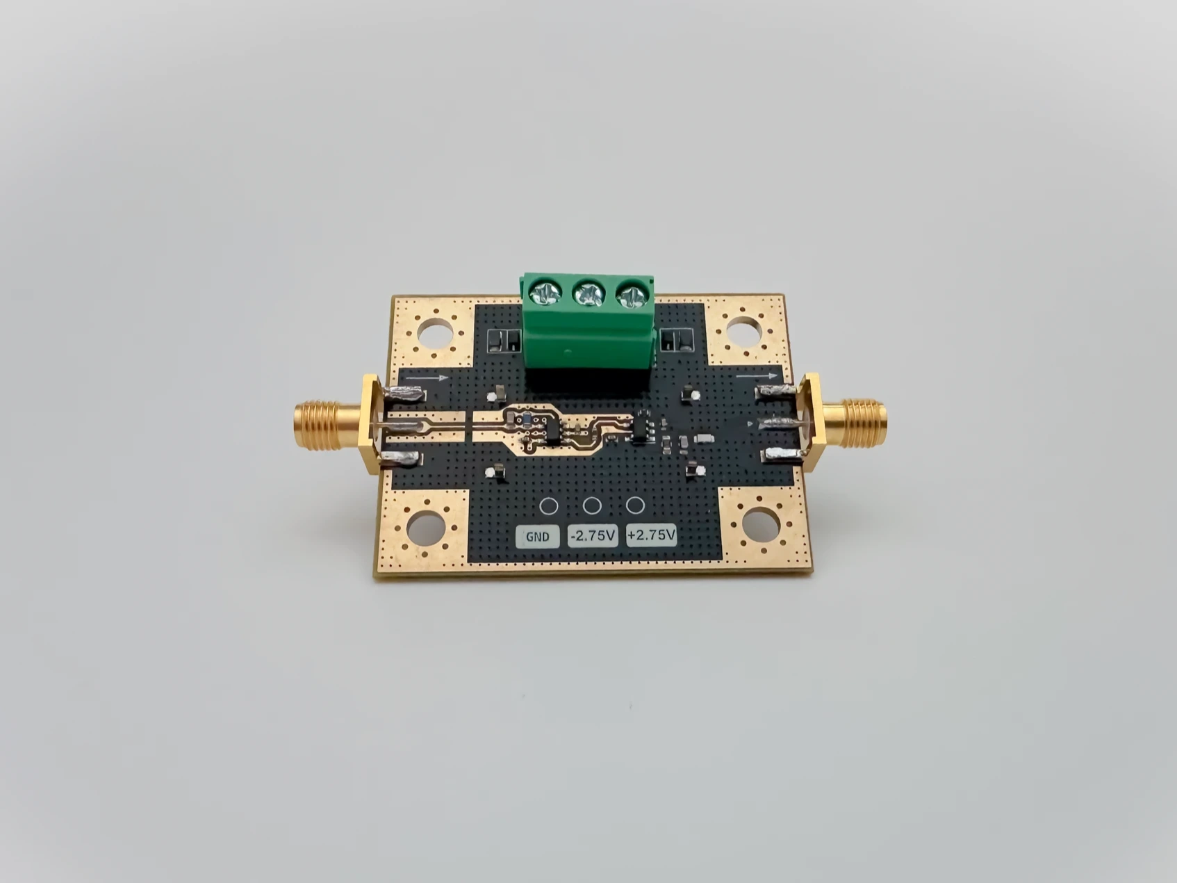
fTIA140-000 Transimpedance Amplifier
Product Overview
The fTIA140-000 is a specialized ultra-low-noise transimpedance amplifier (TIA) module designed to interface directly with high-impedance low-frequency current sources, such as precision photodiodes, chemical sensors, or living biological material.
- The module achieves a total gain of 140 dB with an exceptional input referred current noise of ~600 fA.
- Powering the module requires an isolated dual-rail power supply from ±1.2 V to ±2.75 V.
- The module is of dimensions 50 mm × 37.4 mm (L × W) and features 4 × M4 mounting holes.
- A surface-mount electromagnetic interference (EMI) snap-on shield is included.
Technical Specifications
- Transimpedance gain: 1 MΩ (120 dBΩ)
- 3 dB bandwidth: 16 kHz (Conditions: Cin = 10 pF, Cfeedback = 10 pF)
- Input current range: ±275 nA (Conditions: ±2.75 V rails)
- Input current noise density: 600 fA/√Hz (Conditions: 10.24 kHz, Cin = 10 pF)
- Coupling: DC
- Output impedance: 50 Ω (Type: Series resistor)
- Output stage gain: 10 V/V (20 dB) (Type: Fixed voltage gain)
- Output voltage range: -2.7 V to 2.7 V (Conditions: High impedance)
- Positive supply voltage: 1.2 V to 2.75 V (Relative to GND)
- Negative supply voltage: -2.75 V to -1.2 V (Relative to GND)
- Dimensions: 50 mm × 37.4 mm × 1.6 mm (Custom PCB factor)
- Shielding: Integrated SMT Clips (Optional snap-fit RF shield)
Noise Characterization
https://www.cdn.cerybra.com/tia-noise-recordings-1.png
Figure 1: Noise recordings under Cin = 10 pF load taken from the output of the final gain stage. In order to get back the input referred current density, these values must be scaled by the TIA gain.
Frequency Response
https://www.cdn.cerybra.com/frequency-response-1.png
Figure 2: Frequency response results under Cin = 0 pF load taken from the output of the final gain stage. The final traces are the result of 50 experiment averages. All trials used a chirp source of 100.005 mV amplitude fed through an input 1 MΩ resistor. The ~20 dB reported measurements are relative to the source magnitude, not the true input.
Shipping Terms
Ensure that your shipping information is correct prior to placing an order. We do not assume responsibility for any failure of due diligence on the part of the buyer.
Feedback
All products are tested prior to shipment. If you believe that you have been sent a defective unit, please contact us immediately. If you find any error in the technical specifications, please contact us immediately.